How to Choose the Right PCB Design Software for Your Project

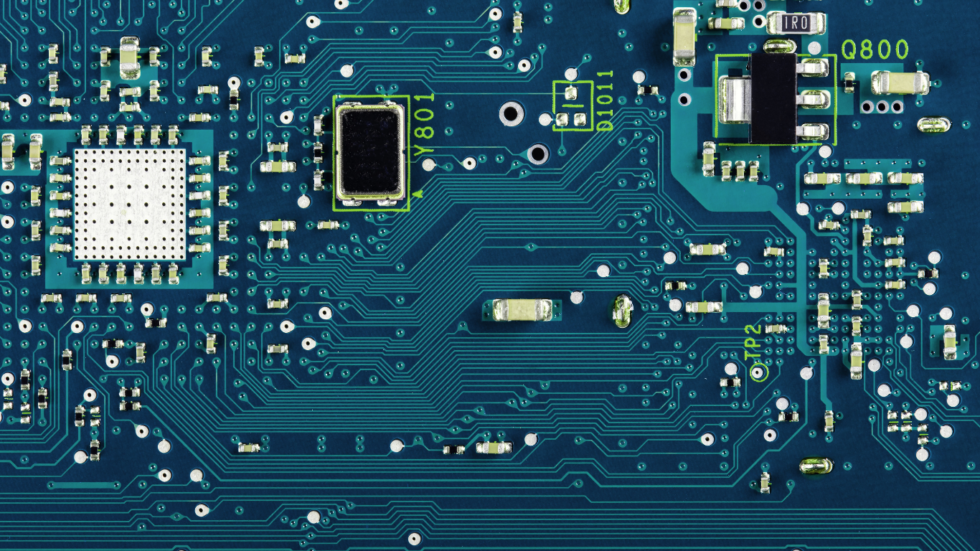
Selecting the best PCB design software is a critical step in ensuring the success of your PCB board design projects. Whether you’re a seasoned professional or just starting, choosing the right software can streamline your workflow, enhance design accuracy, and ultimately produce superior results. This comprehensive guide will help you navigate the selection process by focusing on your project requirements, budget, and skill level, with relevant internal and external resources linked throughout.

1. Assess Your Project Requirements

  • Complexity and Scale: The complexity of your PCB design dictates the level of software you need. For intricate, multi-layer designs, advanced features such as signal integrity analysis and thermal management are essential. Altium Designer is a software that excels in handling complex PCB board design projects. For simpler designs, KiCad might suffice.blue pcb software design
  • Specific Design Rules: Your software should support the specific design rules required for your project, such as spacing constraints, impedance control, and more. Ensuring that your PCB design software aligns with your project’s unique requirements can prevent costly revisions later. For more detailed considerations, refer to our article on Avoiding Common PCB Design Mistakes.

2. Budget Considerations

  • Free vs. Paid Software: Depending on your budget and the complexity of your project, you may choose between free tools like EasyEDA and paid options such as Cadence Allegro. Free software is great for hobbyists or small-scale projects, but for more demanding tasks, investing in professional-grade software is often worth it.
  • Subscription vs. Perpetual Licensing: Consider how long you’ll need the software. Subscription-based models might be more affordable for short-term projects, while perpetual licenses can be more cost-effective for ongoing use. For insights on how we manage different projects within budget, visit our Project Management page.

3. Skill Level and Learning Curve

  • Ease of Use: Beginners might prefer user-friendly software with a gentle learning curve, such as EAGLE, which offers extensive tutorials and a strong user community. As your skills develop, transitioning to more advanced tools like OrCAD can open up more sophisticated design possibilities. Explore our PCB Assembly page to see how we handle the transition from design to production.
  • Support and Community Resources: The availability of robust support and an active user community can significantly ease the learning curve. Software with extensive online resources, such as forums, video tutorials, and user manuals, can help you quickly overcome challenges. Our article on PCB Layout Tips offers practical advice that complements the tools you choose.

4. Key Software Features

  • green pcb design softwareSimulation and Testing Capabilities: Reliable simulation and testing features are essential for verifying that your PCB design will function as intended before moving to production. OrCAD is known for its powerful simulation tools, which are crucial for identifying potential issues early in the design process. To learn more about how we ensure quality in every project, check out our Quality Assurance page.
  • Component Libraries and Third-Party Integration: Access to a comprehensive component library can streamline the design process. Tools like DipTrace offer extensive libraries and easy integration with third-party components, ensuring that you have all the necessary elements at your fingertips. This can be particularly helpful when working on projects that require specialized components.

5. Integration and Collaboration Tools

  • File Compatibility: Ensure that the PCB board design software you choose can handle the file formats your manufacturing partners use. Compatibility with industry-standard formats like Gerber files is non-negotiable for seamless production. For more on how we integrate design and manufacturing, visit our Manufacturing Services page.
  • Collaboration Features: If you’re working with a team, consider software that includes collaboration tools. Cloud-based platforms like Altium Designer allow multiple designers to work on the same project simultaneously, making it easier to manage complex projects. This feature is especially valuable when coordinating between design and production teams.

6. Try Before You Buy

green pcb board design

  • Free Trials and Demos: Before committing to a particular PCB design software, take advantage of free trials and demos to ensure it meets your needs. This hands-on experience is crucial for evaluating usability and features, ensuring that the software you choose is the best fit for your project.
  • Future-Proof Your Choice: Consider how your needs might evolve over time. If you plan to take on more complex projects or scale your operations, choose software that can grow with you. Altium Designer, for instance, offers a range of advanced features that can accommodate increasingly sophisticated designs, making it one of the best PCB design software options for professionals looking to future-proof their capabilities.

Choosing the right PCB design software is a pivotal decision that can influence the success of your projects. By thoroughly evaluating your project requirements, budget, and skill level, you can make an informed choice that ensures a smooth and efficient design process. Check out our PCB Services page for more on how we handle complex designs.

Counterfeit Components – Protecting Your PCBs from Component Fraud

There are many big businesses overseas that have to experience counterfeiting. Just like that electronic parts are also counterfeited by thieves to get huge sums of money in return. The sad reality of getting your PCBs counterfeited is that the user suffers the most after the product designers. It can lead to major troubling situations like affecting your electronic devices including mission-critical military systems like, thermal weapons sights, missile guidance systems, and aircraft.

Just like having fake money in pockets, there are counterfeited electronic components that are no less than to be labeled as fake and are circulating in the market. These components will not only destroy your system but also you’ll lose your money. Although there is no way to check whether a product is free from fraud, you can always have the option to reduce the risk of getting these fake parts to end up in your electronic devices.

Can Counterfeit Components Impact Me?

Most of the time, we do not realize that we have added a defective part or more like a counterfeit component in our device. You can only get to know what happened once you see your system failing brutally in front of your eyes.

To have counterfeit components in your electronic devices can impact your system severely. If you are a company with various projects running – you can lose thousands of dollars only to figure out what part of the device is counterfeited.

This is the reason, we have penned down these five simple ways that can assist you in reducing the risk of getting component fraud. You can easily identify and try to avoid counterfeit electronic components.

1. Source Components From Trusted Vendors

You need to look for trusted vendors to avoid investing in (or say losing money) getting counterfeit components. Ensure to search for a vendor after going through a proper vendor selection process to know the reputable suppliers around you. You can ask the vendors to provide their proven track record with assurance of best quality, reliability transparent sourcing practiced, and more. Give priority to vendors who are a perfect fit according to the approved vendor list and know how to meet the industry standards.

2. Inspect Packaging To Confirm Authenticity

You can look closely for the packaging these counterfeits come in. The thieves who sell such fraudulent products aren’t able to exactly copy the packaging of the original products. This can include spelling mistakes, logo misprinting, irregular serial numbers, or more. So, ensure to check and inspect the visuals of the packaging first to avoid buying these fake items.

3. Run Electrical And Software Tests

Sometimes, just inspecting the packaging of counterfeit components isn’t enough. You also need to make sure to have the necessary tests to figure out which product is fake. To detect whether an electronic part is counterfeited, you need to run software tests and electrical tests like measuring basic parameters including voltage in, voltage out, etc.

4. Perform An X-ray Inspection

An X-ray inspection will let you know the authenticity of an electrical component that you will invest your money in. You can look for various features like die structures, encapsulations, wire bonds, etc. These fake parts are inconsistent with their results, show irregularities, and often have severe defects in them.

5. Exercise Business Caution

You need to be cautious of the unrealistic pricing the vendors offer to you. If you get to see low-price tags on expensive electronic parts, that eventually means the vendor is just looting you by luring you with low prices. Use your intellect to differentiate between the original and fake products.

Final Thoughts

To protect your PCBs from Component fraud, and avoid investing in counterfeit components, follow the five easy ways we have mentioned in this article. Let us know which worked the best for you to identify the fake products. Lastly, it is crucial to stay updated with the latest details regarding counterfeit products – so you can avoid them as much as possible!

Advanced Stack-Up Techniques for Compact PCB Boards

Advanced stack-ups for PCB designs impact the compatibility and reliability of components and connections. Designers achieve high-quality PCB manufacturing by adopting these techniques. These advanced stack-ups not only increase the average life of PCB but also ensure high quality to meet customers’ expectations. Advanced inspection stack-ups like in-circuit testing (ICT) and automated optical inspection (AOI) rectify the defects by early diagnosis. In this blog, we will explore the significance of these techniques in maintaining high-quality PCB boards.

7 Essential Advanced Stack-Up Techniques For PCB Designs

Here, you can get ideas about the usability and cost-effectiveness of advanced stack-ups in designing and manufacturing PCB boards.

Layer Count Approach

Layer count stack-up includes the number of layers to halt the signal and routing errors. Correct configurations of layers enable quality of manufacturing within economical budgets.
Experts in PCB designs recommend four layers of double-sided boards for flexible routing. However, they sometimes recommend six layers to accommodate power distributions and high-speed signals because signal routing is perplexing.

High-Speed Signal Routing Approach

This advanced stack-up ensures a smooth data transmission flow by reducing signals in complex PCB designs. These methods implement differential pairing to match lengths. They trace the complementary signals and maintain signal integrity. You can use microstrip configurations to control electromagnetic interference(EMI) and optimize signal integrity at high speed.

Power Delivery Network Design Technique

This stack-up ensures a stable voltage supply and transparent electronic device operations. A good PDN design ensures the safety of the components. It maintains the power supply points and high voltage disruptions. It locates power ground planes at their proper places. Engineers can reduce loop impedance by suppressing noise and filtering soldering errors.

Thermal Management Approach

The useful life of your PCB boards determines how components and connections are aligned and soldered. Thermal management is the most significant imperative, as it monitors heat moderation. This approach constitutes pathways like thermal vias, heatsinks, and thermal pads. Heat absorption and prevention from the degradation of placed components can be achieved by using these pathways. Advanced thermal managing stack-up can halt heat generation by cooling down the components. The controlled temperature environment avoids heat dissipation and thermal resistance by reducing localized hotspots.

Signal Integrity Stack-up

This advanced stack-up halts signal disruptions by managing electromagnetic interference (EMI). Good signal routing includes signal termination techniques that reduce reflections and crosstalks. In addition, it incorporates ground plane shielding and simulation analysis. The pre-and post-testing of simulations facilitate the evaluation of signal integrity.

Advanced Material Selection Approach

This approach includes laminates, which prevent EMI from being high-speed. Low-loss laminates can avoid the risk of dielectric loss. You can have high-speed PCB boards if your PCB manufacturer uses advanced material selection. This stack-up prevents your PCB from overheating and safeguards the average life of placed components. It monitors thermal conductivity between components and interfaces.

Manufacturing and Assembly Stack-Ups

This stack-up requires compatibility of the manufacturing process with its layout of design.

These stack-ups include identifying debugging points using the built-in self-testing ( BIST) technique. Engineers optimize the layouts by employing copper weight and compartmentalization of components.

The implementation of this stack-up enhances component accessibility. This stack-up permits inspection and prevention techniques to test your PCB boards. Step-by-step inspections of components and connection compatibility reduce post-manufacturing failures. Advanced manufacturing stack-up includes In-circuit testing (ICT) and automated optical inspection (AOI) to detect joint soldering and contamination errors.

Conclusion

In the final analysis, Advanced Stacks Are Required to ensure PCB components’ quality, compatibility, and reliability. They detect errors before they occur and rectify them after the screening and testing phases. Seven essential advanced stack-ups, viability, and feasibility have been described. Thus, a good PCB board should be manufactured after employing these stack-ups for maintenance and quality assurance.

Understanding The Importance Of PCB Layout in Electronics Design

With each passing day, PCB layout keeps evolving with new developments and requirements in electronics. PCB problems like complexity in the dynamics hold great significance in determining the industry’s structure. A PCB, a printed circuit board, has the circuits and components in electronic designs like a canvas. This complex system follows the often-underestimated art and science of PCB layout.

The fundamental importance of PCB layout in electronics design is explored in its key role in shaping electronic device performance, reliability, and manufacturability. From the meticulous placement of components to the complexities of signal routing, let’s examine the critical aspects highlighting the significance of PCB layout in crafting innovative and robust electronic systems.

The Impact Of A PCB Layout On Electronic Design

A PCB layout is the arrangement of components, thoughtful routing of traces, and strategic consideration of power and thermal aspects. It directly impacts electronic performance and determines the overall functionality and reliability of the electronic system. The impact of PCB layout on electronic performance is profound, influencing electronic devices’ functionality, reliability, and efficiency.

Signal Integrity

Guaranteeing consistent signal trace lengths helps maintain signal integrity by preventing timing mismatches. This is crucial for high-speed digital signals to arrive at their destinations simultaneously, minimizing issues like signal skew.

On the other hand, maintaining proper impedance throughout signal traces is also vital. This prevents signal reflections and ensures that the signal arriving at its destination matches the impedance of the receiving component, reducing signal degradation.

However, thoughtful consideration of signal paths involves minimizing crosstalk between adjacent traces and avoiding parallel routing of high-speed and low-speed signals. This helps preserve signal quality, especially in environments where electromagnetic interference (EMI) can be a concern.

Power Distribution

Designing a robust power distribution network involves placing power planes strategically and using low-impedance paths to deliver power efficiently to all components. This minimizes voltage drops and ensures each component receives a stable power supply, preventing performance issues and potential damage.

Thermal Management

The placement of components on the PCB influences their heat dissipation. Grouping high-power components and considering their proximity to heat sinks or thermal vias helps manage temperature effectively.

At the same time, incorporating thermal vias allows heat to dissipate from the components to other layers or external heat sinks. Proper placement and design of these vias are essential to prevent overheating, which could otherwise lead to performance degradation or component failure.

For components that generate significant heat, heat sinks can be crucial—placing these sinks strategically and ensuring a good thermal interface with the components aids in dissipating heat efficiently, maintaining optimal operating temperatures.

Considerations for PCB Layout Designers

The following considerations are important for a PCB layout design process. Designers can enhance the overall performance and scalability of electronic devices. Having an approach helps a robust product and contributes to cost-effectiveness and efficiency throughout the production lifecycle.

Reliability and Robustness

It begins with strategic component placement, where designers aim to minimize thermal stress and enhance overall reliability. Placing components with consideration for heat-producing elements and thermal dissipation holds a balanced thermal profile across the board. Trace routing focuses on creating robust connections. This involves avoiding sharp angles, minimizing the use of vias, and optimizing trace widths to enhance signal integrity and prevent potential points of failure.

EMI/EMC Considerations

Electromagnetic interference (EMI) and electromagnetic compatibility (EMC) require implementing a solid ground plane, which provides a low-impedance return path. Designers must meticulously address signal integrity through shielding techniques and controlled impedance to reduce signal coupling and radiated emissions. Additionally, the strategic integration of filters and ferrite beads helps mitigate EMI issues at their source.

Design for Manufacturability

Efficient and cost-effective production relies on a PCB layout designed for manufacturability. One key aspect is optimizing component placement and orientation to align with automated assembly processes, minimizing the need for user intervention and diminishing the risk of errors during assembly. Using standardized and readily available components simplifies the supply chain, contributing to cost-effectiveness.

Moreover, designers should consider assembly testing during the design phase, incorporating test points and ensuring accessibility for automated testing equipment.

Wrap Up

The precision of PCB layout design wields a profound influence on electronic devices’ reliability, electromagnetic compatibility, and manufacturability. By navigating the intricacies of component placement, addressing EMI/EMC challenges, and embracing manufacturing efficiency, PCB layout designers become architects of not just circuits but resilient and seamlessly producible innovations that power the future of electronics.

The Role of PCBs in IoT Devices: Challenges and Solutions

[et_pb_section fb_built=”1″ admin_label=”section” _builder_version=”4.16″ global_colors_info=”{}”][et_pb_row admin_label=”row” _builder_version=”4.16″ background_size=”initial” background_position=”top_left” background_repeat=”repeat” global_colors_info=”{}”][et_pb_column type=”4_4″ _builder_version=”4.16″ custom_padding=”|||” global_colors_info=”{}” custom_padding__hover=”|||”][et_pb_text admin_label=”Text” _builder_version=”4.24.2″ background_size=”initial” background_position=”top_left” background_repeat=”repeat” hover_enabled=”0″ global_colors_info=”{}” sticky_enabled=”0″]

For the IoT industry, PCBs are the unsung heroes who create functional connections in IoT devices. As the building block of electronic devices, PCBs play an important role in fostering IoT technologies’ efficiency, performance, and reliability. This thin board is made of insulating material with conductive copper track, allowing electronic components to route their connectivity for a circuit.

However, this building block comes with its own set of challenges that we will address so that you can see why your IoT device is acting up. Although these challenges can be a huge hindrance for us, they come with their solutions and an opportunity for us to learn and grow.

Challenges Faced by PCBs in IoT Devices

As IoT aims to connect and network devices, it is on OCB designs to mold how they work.

Size Constraints and Miniaturization

Printed circuit boards (PCBs) face a formidable challenge in IoT due to the devices’ ever-shrinking size requirements. As IoT applications demand increasingly compact and portable solutions, PCBs must grapple with the intricacies of miniaturization. This section explores the impact of size constraints on PCB design, examining the trade-offs between functionality and space efficiency. Strategies such as multi-layered PCBs and surface mount technology will be discussed to address the miniaturization challenge in IoT devices.

Power Consumption Issues

Efficient power management is critical in IoT devices where prolonged battery life and energy conservation are paramount. PCBs face the challenge of optimizing power distribution, minimizing energy loss, and ensuring overall energy efficiency. This segment delves into the intricacies of power consumption challenges, exploring how advanced power delivery systems, low-power components, and intelligent design can mitigate power constraints’ impact on PCBs in IoT applications.

Environmental Factors and Durability

IoT devices often operate in diverse and demanding environments, ranging from extreme temperatures to high humidity or corrosive conditions. PCBs must contend with maintaining functionality and structural integrity under such varied circumstances. This section explores the impact of environmental factors on PCB performance, delving into materials engineering, protective coatings, and design considerations that enhance the durability of PCBs in IoT devices.

Solutions to PCB Challenges in IoT Devices

With these solutions, it is prominent that IoT devices are revolutionizing PCBs’ basic structure and design.

Advanced Manufacturing Techniques

The implementation of advanced manufacturing techniques becomes crucial to address the challenges posed by size constraints and the need for miniaturization in PCBs for IoT devices. This section explores cutting-edge methods such as additive manufacturing, HDI (High-Density Interconnect) technology, and precision assembly processes. By adopting these approaches, engineers can optimize space utilization, enhance component integration, and overcome the limitations associated with the physical dimensions of IoT devices.

Energy-Efficient Design Strategies

Efficient power consumption is a cornerstone in the successful operation of IoT devices. PCBs play a pivotal role in achieving energy efficiency. This segment delves into design strategies that minimize power consumption without compromising performance. Topics include utilizing low-power components, smart power management systems, and implementing energy harvesting technologies. IoT devices can extend battery life and reduce their environmental impact by adopting these energy-efficient design principles.

Materials Innovation for Durability

PCBs must be robustly durable to ensure the longevity of IoT devices. This section explores innovative materials and coating technologies that enhance PCB resilience. A detailed examination of material science solutions will be provided, from corrosion-resistant materials to protective coatings that shield against harsh environmental conditions. By integrating these advancements, PCBs can withstand the rigors of varied environments, ensuring the reliability and durability of IoT devices.

As we delve into these solutions, it becomes evident that the evolution of PCB technology is intricately linked to overcoming the challenges posed by IoT requirements. Integrating advanced manufacturing techniques, energy-efficient designs, and innovative materials is paving the way for more resilient and high-performing PCBs in the rapidly expanding landscape of Internet of Things applications.

Wrapping Up

As we go through these challenges and their recurring solutions, we tend to address the designers’ perspective and also what IoT industries face. On the other hand, this era of innovation demands more user-friendly PCBs so that they can easily be integrated into the devices.

[/et_pb_text][/et_pb_column][/et_pb_row][/et_pb_section]

Printed Circuit Board Assembly (PCBA) Process- A Comprehensive Guide

Have you ever wondered about the structure of electrons that brings your electronic devices to life? Modern electronics have the printed circuit board assembly (PCBA) process that orchestrates this structure, transforming raw components into functional devices. Every electronic device we encounter is connected to the PCB in some way. Everything from smartphones, cars, home appliances, computers, etc., has these electronic building blocks.

Deepening technological advancements and evolving with time, the PCBA process transforms a design into a fully operational circuit. Although it may seem daunting at first, it is quite easy. Before that, you must know about the components used in PCBA.

The Basic Components Of PCB

The PCBA components are essential building blocks that transform a blank circuit board into a functional electronic device. Understanding these components is crucial for anyone delving into the intricate world of Printed Circuit Board Assembly (PCBA). When carefully orchestrated, these elements breathe life into the electronic devices that have become integral parts of our daily lives. Here we tell you about the key elements:

  • Integrated Circuits (ICs)
  • Resistors
  • Capacitors
  • Inductors
  • Diodes
  • Transistors
  • Connectors
  • Resonators and Oscillators
  • Microcontrollers
  • Sensors

The PCBA Process Steps

Step 1. Design and Layout

The Design and Layout phase of the Printed Circuit Board Assembly (PCBA) process is the foundational stage where the blueprint of the circuit board comes to life. Designers utilize specialized software, typically CAD (Computer-Aided Design), to meticulously plan the placement of components, signal traces, and layers. This step is pivotal in ensuring optimal functionality, as a well-thought-out design directly impacts the efficiency and manufacturability of the PCB. Designers must carefully consider factors like signal integrity, thermal management, and electromagnetic interference, laying the groundwork for the subsequent stages of the PCBA process.

Step 2: Fabrication of PCB

Fabricating a PCB involves transforming the design into a tangible board. This step includes selecting appropriate substrate materials, commonly fiberglass reinforced with epoxy and copper foils for the conductive layers. The fabrication process employs techniques like etching, layering, and coating to create the final PCB. The precision and quality of fabrication significantly influence the overall performance and reliability of the electronic device.

Step 3: Component Placement

Determining how components will be placed on the PCB is critical in the PCBA process. Engineers must choose between automated assembly machines or manual labor for precise component placement. This step’s precision is crucial as it directly affects the final electronic device’s functionality and efficiency. Careful consideration is given to optimizing the use of space on the PCB.

Step 4. Soldering

Soldering is the process that brings the PCB to life by creating electrical connections between components and the board itself. There are two primary techniques: Surface Mount Technology (SMT), where components are mounted directly onto the PCB surface, and Through-Hole Technology (THT), where components are inserted into drilled holes on the PCB. Reflow soldering, a common method, involves melting solder to form secure connections. The success of the soldering step ensures the reliability of the entire PCBA.

Step 5: Inspection and Testing

After assembly, thorough inspection and testing are crucial to guarantee the quality and functionality of the PCB. Visual inspection, automated optical inspection (AOI), and X-ray testing are common quality control measures. Functional testing ensures that the assembled PCB meets performance specifications, identifying and rectifying any defects before the final product reaches the end-user.

Step 6: PCB Design Considerations

PCB Design Considerations encompass the principles and guidelines that govern the layout, trace routing, and component placement during the design phase. These considerations are essential for achieving optimal performance, signal integrity, and reliability in the final product. Factors influencing design include the type of electronic components, the intended application, and the overall goals of the electronic device.

Step 7: Fabrication of PCB

Fabricating a PCB involves transforming the design into a tangible board. This step includes selecting appropriate substrate materials, commonly fiberglass reinforced with epoxy and copper foils for the conductive layers. The fabrication process employs techniques like etching, layering, and coating to create the final PCB. The precision and quality of fabrication significantly influence the overall performance and reliability of the electronic device.

Step 8: Component Placement

Determining how components will be placed on the PCB is critical in the PCBA process. Engineers must choose between automated assembly machines or manual labor for precise component placement. The precision of this step is crucial as it directly affects the functionality and efficiency of the final electronic device. Careful consideration is given to optimizing the use of space on the PCB.

Step 9: Soldering Techniques

Soldering techniques are integral to the PCBA process, determining how components are securely connected to the PCB. Surface mount technology (SMT) involves mounting components directly onto the PCB surface, while through-hole technology (THT) involves inserting components into drilled holes on the PCB. Reflow soldering, a widely used technique, melts solder to form reliable connections, ensuring the electronic device’s durability and performance.

Step 10: Inspection and Testing

Inspection and Testing are critical steps to verify the quality and functionality of the assembled PCB. Various quality control measures are employed, including visual inspection, automated optical inspection (AOI), and X-ray testing. Functional testing ensures that the PCB meets specified performance criteria, identifying and rectifying any defects before the final product reaches the end-user.

The PCBA process is a multifaceted journey from design to a fully operational circuit. Each step plays a role in ensuring the final electronic device’s functionality, reliability, and performance. As technology advances, the PCBA process evolves, presenting new opportunities and challenges for electronic manufacturers.

Common PCB Manufacturing Challenges and Their Solutions

The printed circuit board, PCB, bridges the gap between signals and powers. It makes sure power is directed within electronic devices. These fundamental components are often overlooked in sleek devices. Power is the backbone of connectivity and functionality. However, designing a PCB and making it fully functional can sometimes leave loopholes. These loopholes generate challenges that are caused during the manufacturing phase but show their failure during assembly.

The entire manufacturing of PCBs is riddled with challenges, including the delicate placement of minuscule components, the strategic management of heat, and the selection of materials resilient to diverse environmental factors. But with every challenge comes the solution, and if we fail to find it, we will jeopardize the performance and efficiency of electronic devices.

8 PCB Manufacturing Challenges And Solutions

While dissecting the routes of these challenges, we have curated a set of solutions from industry experts. Addressing these challenges isn’t just a matter of technical finesse; it is a strategic imperative. The smooth functionality of electronic devices hinges on successfully navigating these hurdles. Read on to learn more about the key challenges and the possible solutions.

Design For Manufacturability DFM

Design for Manufacturability (DFM) is a cornerstone for efficient PCB production. Ensuring that the design is conducive to manufacturing is vital in avoiding bottlenecks and errors. Challenges may arise when intricate designs pose component placement or thermal management difficulties. Solutions involve collaborative efforts between designers and manufacturers, incorporating DFM principles early in the design phase to optimize efficiency, reduce costs, and enhance overall manufacturability.

Solder Quality Control

The integrity of solder joints is paramount for the reliability of a PCB. Maintaining consistent solder quality can be challenging, leading to poor connections and premature component failure. Implementing rigorous quality control measures, including visual inspections and automated testing, is essential. Utilizing advanced soldering technologies and adhering to industry standards further ensures the production of PCBs with robust and reliable solder joints.

Slivers

Slivers, minute slivers of copper or other materials between traces, pose a challenge in PCB manufacturing, potentially causing short circuits or signal interference. Precision and thorough inspection are critical to identifying and eliminating slivers. Latest atest manufacturing methodsmethods , such as laser cutting and high-precision etching, help minimize the occurrence of slivers and ensure the integrity of the PCB design.

Missing Solder Masks

The absence of solder masks can result in bridging between solder joints, compromising the PCB’s functionality. Detecting and rectifying missing solder masks requires meticulous inspection and adherence to quality control protocols. Automated inspection systems and the careful application of solder masks during manufacturing are pivotal in preventing and addressing this challenge.

Acid Traps

Acid traps, where etching solutions can become trapped during manufacturing, threaten the
PCB’s integrity. This challenge can lead to uneven copper traces or other structural issues. Implementing effective rinsing and quality control processes in the manufacturing line helps mitigate acid traps, ensuring a clean and uniform etching process.

Material Defects

Material defects, such as inconsistencies in substrate materials, can compromise a PCB’s overall performance and reliability. Thorough material testing and quality assurance procedures are essential to identify and address these defects. Collaborating with reputable material suppliers and maintaining stringent quality control measures in the manufacturing facility are key strategies for minimizing material-related challenges.

BGA Spacing

Ball Grid Array (BGA) components present a specific challenge in PCB manufacturing due to their densely packed nature. Inadequate spacing can lead to issues during soldering and compromise the reliability of the connections. Precision in BGA component placement, utilizing advanced soldering techniques, and implementing thorough inspection processes are crucial for overcoming spacing challenges and ensuring the integrity of BGA connections.

Test Point Existence

Test points are essential for diagnosing and troubleshooting PCBs during and after manufacturing. The challenge is ensuring that these test points exist and are accessible. Incorporating standardized test point designs, strategically placing them on the PCB, and employing automated testing procedures contribute to overcoming this challenge, facilitating efficient testing and quality assurance throughout the manufacturing lifecycle.

Conclusion

There you go! By understanding the intricacies of PCB manufacturing challenges and proactively seeking solutions, manufacturers can ensure the reliability and quality of their products and position themselves at the forefront of technological advancement.

Advancements in Materials – Explore Latest in PCB Substrates

While traditional materials have served as the backbone of PCBs, a closer examination reveals inherent limitations and challenges. Understanding these constraints sets the stage for exploring cutting-edge solutions. The heart of innovation lies in printed circuit boards (PCBs) for the electronics industry. Within this dynamic industry, the substrates that underpin PCBs have emerged as a focal point of exploration and advancement. PCB substrates have moved from the foundations of traditional materials to the noncomposite wonders. By discussing how these advancements are reshaping industries and propelling us into an era of unprecedented electronic possibilities, we will know how to take leverage of this advancement.

What Are PCB Substrates?

Printed Circuit Board (PCB) substrates are the foundational materials that provide mechanical support and electrical insulation for the components on a PCB. These substrates serve as the base upon which the conductive paths and electronic components are mounted. Typically composed of insulating materials, PCB substrates play a crucial role in supporting the conductive traces that facilitate the flow of electrical signals throughout the circuit.

The choice of substrate material is vital, influencing the board’s performance, reliability, and overall functionality. Common materials used for PCB substrates include fiberglass-reinforced epoxy laminates (FR-4), which are widely employed in conventional PCBs, and more advanced materials like flexible polymers or ceramics for applications requiring flexibility or high-frequency performance.

Latest Innovations in PCB Substrates

PCB substrates provide a platform for the intricate interconnection of electronic components, enabling the creation of complex circuits that power a diverse array of electronic devices, from smartphones to industrial machinery. The continual innovation in PCB substrate materials contributes to the ongoing evolution of electronic technology, allowing for improvements in performance, miniaturization, and the development of new functionalities.

High-Frequency Materials

High-frequency materials represent a significant stride in the evolution of PCB substrates, particularly in response to the demands of new tech such as 5G communication. These materials exhibit low signal loss and enhanced signal integrity, crucial for transmitting data at higher frequencies. Common high-frequency substrate materials include polytetrafluoroethylene (PTFE) and ceramic-filled hydrocarbons. Adopting these materials enables the design of PCBs capable of supporting the rapid data rates required for next-generation wireless communication and other high-frequency applications.

Flexible and Rigid-Flex Substrates

The advent of flexible and rigid-flex substrates marks a departure from the rigid confines of traditional PCBs. Flexible substrates, often composed of polyimide, allow PCBs to bend or conform to non-planar surfaces, opening up new possibilities for wearable devices and unconventional form factors. Rigid-flex substrates combine flexible and rigid materials in a single board, balancing adaptability and structural integrity. This innovation is reshaping the design landscape, enabling the creation of foldable smartphones, flexible displays, and other compact electronic devices.

Nanocomposite Materials

Nanocomposite materials revolutionize PCB substrates by incorporating nanoparticles into the base material. These nanoparticles, often carbon-based, enhance mechanical strength, thermal conductivity, and electrical properties. The resulting PCBs exhibit improved performance, reduced size, and increased reliability. Nanocomposites are especially valuable in applications where size and weight are key factors, such as aerospace and medical devices. As technology advances, integrating nanocomposite materials into PCB substrates propels electronic devices into realms of previously unimaginable efficiency and capability.

Final Thoughts

Exploring the latest innovations in PCB substrates reveals a tapestry of technological breakthroughs poised to redefine electronic devices’ capabilities and design possibilities. The convergence of high-frequency precision, flexible adaptability, and microscopic enhancements of nanocomposite materials underscores the dynamic nature of electronic engineering. It sets the stage for a future where devices are interconnected and optimized for efficiency, performance, and versatility.

As we stand on the brink of this transformative era, the journey through these innovations in PCB substrates signals progress and a profound leap forward into the next generation of electronic design and functionality.

A Beginner’s Guide to Circuit Board Assembly

You may not realize it, but printed circuit boards are more important and common than you think. Present within a vast majority of the electronic devices we use daily, these circuit boards are a vital component that ensures the proper functionality of electronics.

Keeping this in mind, it is essential to understand that the assembly of these circuit boards is vital, primarily because they are a major component within electronics.

Because of the components and circuitry involved within an average PCB, the manufacturing process is incredibly complex.

Not only that, but the board you are working on also needs to be reliable enough to support the assembly process so that the resulting PCB does not turn out to be faulty.

Let us discuss this in further detail, exploring deeper into the concept of PCB assembly, understanding the resources needed, and the assembly process itself.

PCB Assembly: In Depth

Before going into the specifics of the overall process, let us first establish a foundation: the assembly process, taking a broader look at this part of PCB development.

Simply speaking, the initial state of a circuit board that has yet to go through any component installation is a printed circuit board, also known as the PCB.

When the necessary electrical components have been installed onto the board, the resulting circuit board that we end up with is called the printed circuit board assembly, otherwise known as a PCBA.

Many people consider the PCB assembly and manufacturing process as the same thing, but that is not the case.

The main reason why assembling the circuit board is different is that when the PCB is being manufactured, it goes through a selection of different catering to the design and creation of the board.

However, assembly is what comes after the board has been developed after going through the design phase, involving the assembly of the electronic parts according to the main function of the PCB.

Resources Needed for PCB Assembly

Some certain tools and components are required to ensure that the overall assembling of the PCOB goes smoothly, and these include:

  • The printed circuit board itself
  • Transistors and other basic electronic components
  • A soldering flux
  • Necessary tools to perform a solder, including a soldering wire, soldering iron, and testing equipment.

Different Techniques of PCB Assembly

Even though the through-hole insertion technique for applying electrical components was the only way to develop PCBs, technological advancements have led to other methods, such as assembling a circuit board through SMT.

Assembling Using Thru-Hole Components

This type of PCB assembly involves certain components with wiring coming out of them, which go through the tiny holes within the PCB and are soldered.

When assembling a PCB using thru-hole components, it goes through a process called wave soldering, which involves the being applied in the form of a solder bar, which is put in an incredibly hot bath. This high temperature makes the solder stay molten and creates a wave-like design.

Once the wave has been made, the electrical components are passed through the molten state to be fitted within their places.

The overall assembling and solder process for these components includes:

  • Insertion of the necessary electronics
  • Applying the solder flux
  • Preheating the solder bar
  • Creating the wave solder
  • Cleaning and inspecting the PCBA
  • Testing the final product

Assembly Using SMT

Also known as surface mounting technology, this assembly process involves special components that do not contain any leads and do not need to go through any holes to be soldered.

Using this technology, they are directly soldered onto the PCB and are highly compatible with automation, leading to machinery automating the entire assembly process.

Conclusion

Many factors need to be considered when assembling a printed circuit board. However, with the right tools and components, you will not face any problems if you follow the steps mentioned above to assemble a PCB.

RoHS Compliance and Lead-Free Soldering Techniques

One of the significant steps towards achieving environmental responsibility was the introduction of RoHS compliance regulations. RoHS, which stands for Restriction of Hazardous Substances, is a directive aimed at reducing the use of hazardous materials in electrical and electronic equipment. This directive has driven the adoption of lead-free soldering techniques in electronics manufacturing. In this article, we will explore RoHS compliance, its significance, and the lead-free soldering methods that have become central to it.

RoHS Compliance: A Brief Overview

The RoHS directive, formally known as Directive 2011/65/EU, originated in the European Union but has had a global impact on the electronics industry. Its primary objective is to restrict the use of specific hazardous substances in electronic and electrical equipment. These substances include:

  • Lead (Pb)
  • Mercury (Hg)
  • Cadmium (Cd)
  • Polybrominated biphenyls (PBB)
  • Hexavalent chromium (Cr6+)
  • Polybrominated diphenyl ethers (PBDE)

The RoHS directive applies to a wide range of electronic products, from household appliances to industrial machinery. Manufacturers and suppliers must comply with RoHS regulations to market their products in the EU and other regions that have adopted similar standards.

The Significance of RoHS Compliance

RoHS compliance carries several significant advantages and benefits, both for the environment and for consumers:

  • Environmental Impact

By restricting hazardous substances, RoHS helps reduce the environmental footprint of electronics manufacturing. It limits the release of toxic materials into the environment, thereby mitigating potential harm to ecosystems and human health.

  • Product Safety

RoHS compliance ensures that electronic products are safer for consumers. It reduces the risk of exposure to hazardous substances, particularly in consumer electronics and appliances that may come into direct contact with people.

  • Recycling and Disposal

RoHS-compliant products are easier to recycle and dispose of responsibly. They contain fewer hazardous materials, making them safer for recycling and preventing the contamination of landfills.

  • Global Market Access

Compliance with RoHS regulations enables manufacturers to access global markets. Many countries and regions outside the EU have adopted similar standards, making RoHS compliance essential for international trade.

Lead-Free Soldering Techniques

One of the most significant changes driven by RoHS compliance is the shift from lead-based solder to lead-free solder in electronics manufacturing. Lead-free soldering techniques have become central to achieving RoHS compliance. Here are key aspects of lead-free soldering:

1. Composition

Lead-free solder alloys are typically composed of various metals, with tin (Sn) being the primary component. Common alloys include Sn-Ag-Cu (SAC), Sn-Cu, and Sn-Ag. These alloys offer comparable or even superior mechanical and electrical properties to traditional lead-based solder.

2. Soldering Temperature

Lead-free soldering often requires higher temperatures than lead-based soldering. This can necessitate adjustments in soldering equipment, such as reflow ovens and soldering irons, to accommodate the higher melting points of lead-free alloys.

3. Compatibility

When transitioning to lead-free soldering, it’s essential to ensure that all components and materials used in the assembly process are compatible with lead-free solder. Some components may require adjustments or alternative materials.

4. Solder Paste and Flux

Lead-free solder paste and flux materials are formulated to work with lead-free solder alloys. These materials play a crucial role in ensuring proper wetting and bonding during the soldering process.

5. Process Control

Control over the soldering process is vital to achieve consistent and reliable solder joints. Manufacturers must fine-tune their soldering profiles to account for the characteristics of lead-free solder, ensuring proper reflow and minimizing defects.

Benefits of Lead-Free Soldering

The adoption of lead-free soldering techniques offers several benefits beyond RoHS compliance:

  • Environmental Responsibility

Lead-free solder reduces the environmental impact of electronics manufacturing by eliminating a highly toxic substance.

  • Health and Safety

Lead-free solder is safer for both manufacturing personnel and end-users, reducing the risk of lead exposure.

  • Recycling

Lead-free solder makes recycling and disposal of electronic products more environmentally friendly.

  • Global Market Access

Lead-free soldering techniques enable manufacturers to access global markets, ensuring their products comply with various environmental regulations.

  • Mechanical Strength

Lead-free solder alloys often exhibit improved mechanical strength, enhancing the reliability of soldered joints.

Conclusion

RoHS compliance and the adoption of lead-free soldering techniques have transformed the electronics manufacturing industry, promoting environmental responsibility, product safety, and global market access. While the transition to lead-free soldering presents challenges, the long-term benefits in terms of sustainability and safety make it a crucial step towards a more responsible and sustainable electronics industry. As technology continues to advance, ongoing research and development will further enhance lead-free soldering techniques, making them even more efficient and eco-friendly.